COMPANY

About VeriSilicon
Executive Team
Press Release
In the News
Events
Partners
Careers
Trademark
Contact Us

INVESTOR RELATIONS

Board of Directors
Major Investors
Stock Information
IR Contacts

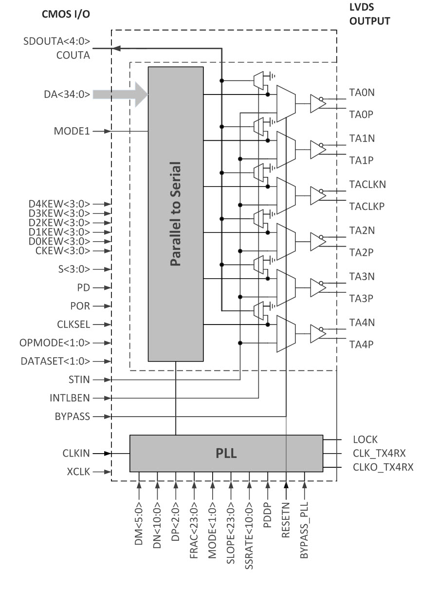
The LVDS transmitter is designed to support Single Link transmission between Host and Flat Panel Display with up to SXGA+ resolution and Dual Link transmission between Host and Flat Panel Display with up to UXGA resolution.

The IP converts 35-bit of CMOS/TTL data into LVDS data stream. The transmitter can be programmed for rising edge or falling edge clocks via a dedicated pin.

Features

  • Silicon Proven in 22,28,55,65,130n,180n from SMIC, Global Foundries and Samsung

  • Compatible with the National DS90CF386

  • Compatible with the TIA/EIA-644 standards

  • Converts 35 bits data to 5-pair LVDS data stream

  • Supports up to 1.05Gbps data rate for UXGA                 

  • Clock edge selectable

  • Wide dot clock range: 25 ~ 150MHz suited for VGA, SVGA, XGA, SXGA, SXGA+ and UXGA

  • Output range is changeable from 50mV to 400mV

  • Core area: 0.5430mm^2

  • Power consumption:

    -  175.4mW@1.05Gbps, prbs7 pattern

LVDSTX_PHY.jpg

Search

Contact

Language

简体中文

English

日本語

芯原股份 (688521.SH)
Thank You for Subscribing
Thank you for subscripting to receive the latest news of VeriSilicon via email .
While you await our next issue, we invite you to learn more about VeriSilicon through the resources below.
CUSTOM SILICON SERVICE
Embedded Vivante GPU, Vision, and IoT cores
Embedded Vivante Dedicated Vision IP
ZSP Digital Signal Processors
Hantro Video Encoder and Decoder IP
Company Information
Close