公司

关于芯原
管理团队
新闻发布
公司动态
市场活动
合作伙伴
加入我们
商标
联系我们

投资者关系

董事成员
主要投资者
股票信息
投资者联系
企业社会责任报告

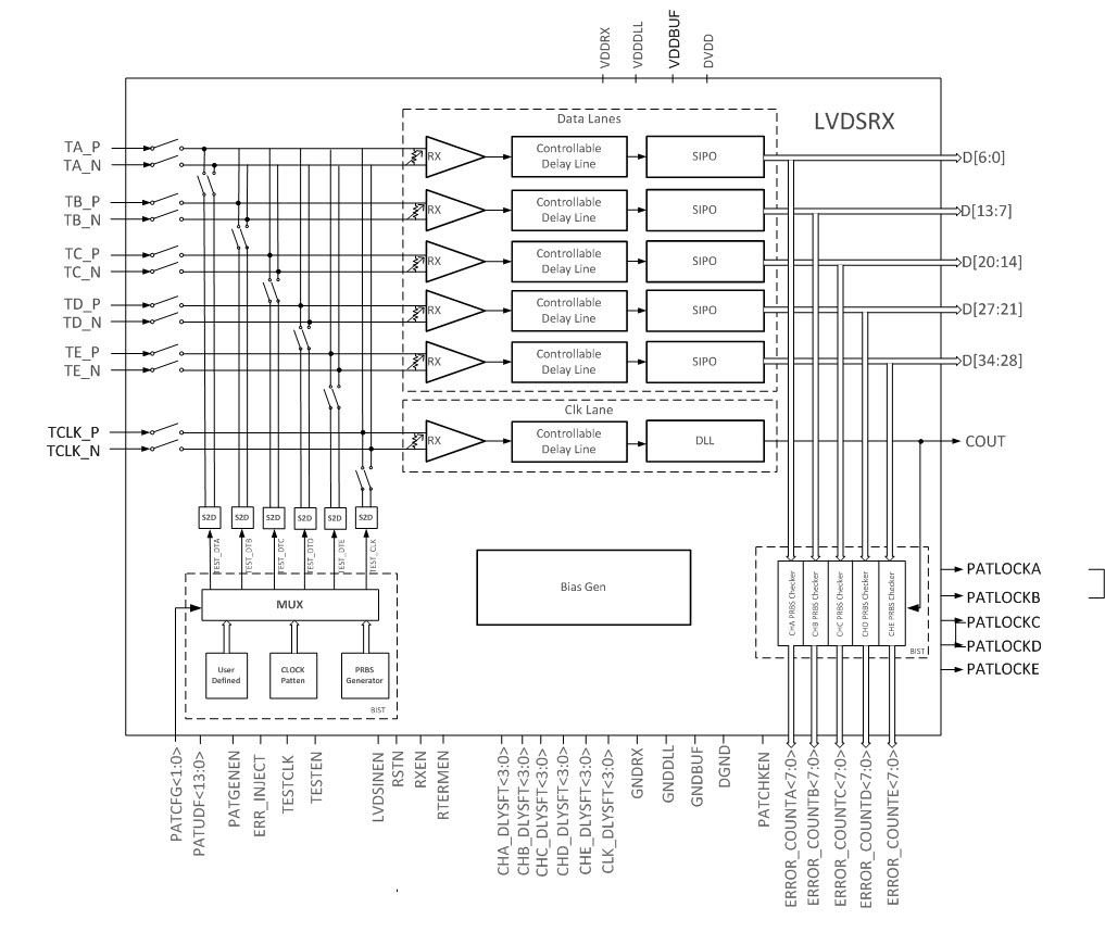
The LVDS Receiver IP is designed to support Single Link transmission between Host and Flat Panel Display with up to SXGA+ resolution. The LVDS Receiver IP converts the LVDS data stream back into 35 bits of CMOS data with a variety of LCD panel controllers.

The receiver LVDS clock operates at rates from 25 MHz to 150 MHz, At an incoming clock rate of 150MHz, each LVDS input line is running at a bit rate of 1.05Gbps.

Features

  • Converts 5-pair LVDS data stream into parallel 35 bits of CMOS data

  • Compatible with the TIA/EIA-644 LVDS standards

  • Supports up to 1.05Gbps data rate for UXGA

  • On-chip DLL requires no external component

  • Power-down control function

  • Negative clock edge for data output

  • Core area: 0.4134mm^2

  • Wide dot clock range: 25 ~ 150MHz suited for VGA, SVGA, XGA, SXGA, SXGA+ and UXGA

  • Function compatible with the National DS90CF386

  • Silicon Proven in 22,28,55,65,130n,180n from SMIC, Global Foundries and Samsung

  • On chip 100Ω termination resistor. Can be disable.

  • Power consumption:

    -  71.8mW@1.05Gbps, prbs7 pattern

LVDSRX_PHY.jpg

搜索

联系

语言

简体中文

English

日本語

芯原股份 (688521.SH)
感谢您的订阅
感谢您通过邮件.订阅芯原的最新消息。在您等待我们网站的下次更新时,我们邀请您通过以下资源来了解芯原的更多信息。
一站式芯片定制服务
Vivante图形处理器IP
Vivante神经网络处理器IP
ZSP数字信号处理器IP
Hantro视频处理器IP
关于芯原
关闭